


The Story
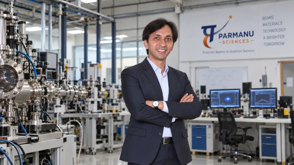
India's semiconductor story is usually told through fabs, chip design and investment commitments. Behind every advanced chip, though, sits a layer that gets almost no attention: the machines that manipulate materials at atomic scale. New Delhi-based Parmanu Sciences is a deep-tech company and DPIIT-recognised startup developing an indigenous accelerator and ion-beam platform, with semiconductor ion implantation as its initial target application.
The machine in question is an ion implanter. It takes atoms of a chosen element, strips them of electrons to create charged ions, accelerates them through electric and magnetic fields, and drives them into a silicon wafer where they settle beneath the surface. Those implanted atoms change how electricity behaves in that region: boron creates p-type areas, phosphorus or arsenic create n-type ones. The ion species determines what goes in, the energy determines how deep, and the dose determines how much. It is, in effect, a machine for writing electrical properties into silicon, and a modern chip process can need dozens of implantation steps.
Parmanu comes at that from an accelerator-engineering foundation rather than from semiconductor equipment. Instead of treating implantation as a black-box tool, it works across the underlying stack: ion generation, acceleration, beam transport, focusing and steering, vacuum, diagnostics and target delivery. The development work so far runs to engineering drawings, simulations and beamline hardware built in India. The objective is to turn that base into a dedicated ion-implantation platform able to handle different ion species, rather than a machine designed around a single use case.
The team is where the specifics sit. Founder Sahil Pershad has spent 21 years in the particle accelerator field across accelerator systems, beamlines and scientific instrumentation, including work as an Indian representative and system integrator for European accelerator suppliers such as the Italian synchrotron facility Elettra Sincrotrone Trieste. Rajan Joshi brings 33 years across BARC, DRDO and the Inter-University Accelerator Centre in New Delhi, covering heavy-ion accelerators, ion implantation, LINAC systems and high-voltage engineering. Rajeev Ahuja brings 35 years at IUAC in mechanical engineering, vacuum systems, and the design and fabrication of accelerator components. The wider team covers beamline simulation, ion-source operation, mechanical design, vacuum engineering, electronics and instrumentation, with experience extending to hardware for space payload programmes.
Parmanu is also in the final stages of a technology transfer covering an indigenous high-performance ion source. Integrating it would give the company control over one of the fundamental building blocks of ion-beam generation.
The policy backdrop is genuine. Semicon 2.0, approved in July 2026 with an outlay of ₹1,27,500 crore, names semiconductor equipment and materials among its strategic pillars rather than treating fabs alone as the objective. Twelve projects have been approved with committed investments above ₹1.64 lakh crore.
A production-qualified semiconductor implanter is still ahead of the company rather than behind it, and funding and customer details have not been disclosed.
Why It Matters
The gap Parmanu has identified is real, and it is worth stating clearly before picking at the numbers around it.
India has spent three years attracting semiconductor investment and has been reasonably successful at it. What it has not done is build the layer underneath. A fab is an assembly of several hundred extraordinarily precise machines, almost none of which India makes. Lithography comes from the Netherlands and Japan, deposition and etch from the United States, implantation from a handful of American and Japanese suppliers. A country can host a fab and still own none of the technology inside it, which is the difference between being a manufacturing location and having an industrial base. Semicon 2.0 naming equipment and materials as strategic pillars is an acknowledgement of exactly that.
Ion implantation is a sensible place to attack it. Unlike extreme ultraviolet lithography, which is effectively unreachable, an implanter is an accelerator: an ion source, an acceleration stage, beam optics, a vacuum system and a control layer. Those are disciplines India actually has, developed over decades at the Inter-University Accelerator Centre, BARC, RRCAT and the Variable Energy Cyclotron Centre. The engineering is hard but it is not foreclosed.
And this is where the team matters more than the thesis. Joshi's 33 years span BARC, DRDO and IUAC, covering heavy-ion accelerators, ion implantation and high-voltage engineering. Ahuja's 35 years at IUAC cover vacuum systems and the fabrication of accelerator components. Those are not adjacent credentials; they are the exact disciplines an implanter is assembled from, earned at the institutions where India's accelerator knowledge actually lives. A company proposing to build an ion-beam platform in India with people from IUAC and BARC is a materially different proposition from one proposing it without them.
The founder's background fits that reading. Earlier work included representing and integrating accelerator systems for Indian users, which is genuine domain access: knowing what the equipment costs, who buys it, how it is specified and where it fails. The technical experience extends into beamline design, simulation and physical beamline systems developed in India. Parmanu is not presenting integration as equivalent to having built a production accelerator. It is using an accelerator-engineering base to develop a proprietary ion-beam platform.
The deeper argument, that precision control of ion beams is a reusable capability rather than a single product, holds up on its own terms. The same core disciplines, ion generation, acceleration, beam transport, vacuum and diagnostics, can be engineered for different particles, energies and targets. That makes the underlying capability genuinely reusable across specialised research and industrial applications, even though each end product would require its own engineering and qualification.
The Strategic Read
Start with the market size, because the numbers usually attached to this pitch are the wrong ones.
SEMI forecasts all semiconductor manufacturing equipment at $165.9 billion in 2026, reaching $229.5 billion by 2028. Those are the figures that circulate whenever an equipment company raises money in India, and they describe lithography, deposition, etch, metrology, cleaning, test and everything else. Ion implantation is a narrow slice. Independent estimates put the global implanter market between roughly $1.8 billion and $3.1 billion for 2026, and the cleanest single data point is Axcelis, the only listed pure-play ion implantation company, which reported about $1 billion of revenue in 2025. The addressable market is a few billion dollars, not a few hundred billion, and any assessment of this opportunity has to start from the smaller number.
The second point concerns India specifically. Ion implantation is a front-end wafer process. It happens in a fab, not in a packaging plant. The large majority of India's approved semiconductor projects are assembly, testing, marking and packaging facilities, which do not use implanters. The domestic customer base for a production implanter is therefore not twelve projects and ₹1.64 lakh crore; it is the small number of actual front-end fabs, chief among them Tata Electronics and PSMC at Dholera. That is a short list of buyers, each of which will take years to qualify a new tool.
The competitive structure compounds it. Ion implantation is supplied by a tight oligopoly: Applied Materials, Axcelis, Nissin Ion Equipment, Sumitomo Heavy Industries Ion Technology, ULVAC, Ion Beam Services and China's Kingstone. Fabs qualify implanters over years, because a beam that drifts out of specification scraps wafers worth more than the machine. No fab manager buys an unproven implanter to save money. The nearest precedent for what Parmanu is attempting is Kingstone, built to serve Chinese domestic fabs with substantial state support behind it, and that took a decade.
The optionality argument has two halves worth separating. An ion-implantation platform does not automatically become an accelerator-driven nuclear system, a neutron capture therapy facility or a fusion materials rig. Each needs different engineering, infrastructure, qualification and regulation. What remains true after that qualification is narrower but real: expertise in ion sources, beam transport, vacuum systems and diagnostics is genuinely reusable, and in India it is scarce. The list of downstream applications is a direction of travel. The underlying engineering capability is the asset.
Which points to a possible first market beyond production fabs. Research institutions, universities, materials laboratories and specialised industrial users buy ion-beam and accelerator systems in low volumes, and their qualification bar is a working instrument rather than a zero-defect production tool. Deployments there would build manufacturing capability, field data and customer credibility while the company works toward the far higher requirements of a semiconductor fab. It is also the market this team already knows, having spent decades inside the institutions that make up its customer base.
What remains to be demonstrated is the transition from engineering capability to a repeatable, manufacturable and eventually fab-qualified tool. That is a different discipline from designing a beamline: it is process control, yield, service response, spare parts and the ability to prove a machine behaves identically on its two hundredth wafer as on its first. Funding, team scale, customer traction, validation results and deployment milestones are the measures that will matter from here. The engineering base is the starting point. Industrialisation and qualification are the work.
For daily, sharp analysis of the biggest moves in the Indian business and startup ecosystem, follow StartupFox.